Mainboard Revisions
- Table of contents
- Mainboard Revisions
Board design and schematics
for Rev1
PDF of the schematics: https://github.com/LaosLaser/Hardware/tree/master/laos-board-rev1/output/pdf/laos-board.pdf
PDF of the board: https://github.com/LaosLaser/Hardware/tree/master/laos-board-rev1/production/PI_E382816.pdf
for Rev2
PDF of the schematics: https://github.com/LaosLaser/Hardware/tree/master/laos-board-rev2/output/pdf/laos-board.pdf
PDF of the board: https://github.com/LaosLaser/Hardware/tree/master/laos-board-rev2/production/PI_E404084.pdf
for Rev3
PDF of the schematics: https://github.com/LaosLaser/Hardware/tree/master/laos-board-rev3/output/laos-board-rev3.pdf
PDF of the board: https://github.com/LaosLaser/Hardware/tree/master/laos-board-rev3/production/PI_E453774.pdf
for Rev4
SVG of the schematics: https://raw.github.com/LaosLaser/Hardware/master/laos-board-rev4/laos-board.svg
SVG of the board: https://raw.github.com/LaosLaser/Hardware/master/laos-board-rev4/laos-board-brd.svg
Known bugs
Known bugs in Rev1
These bugs are only relevant to board version 0.1.
Pololu microstep problem
The microstep step settings does not work as expected. If you mount all the jumpers, and the motors are still making full-steps, instead of 1/16steps, this is caused by incorrect resistor values.
R6, R11, R14, R20: '''use 1K resistors''' instead of the 10K resistors mentioned in the schematics.
SD socket problems
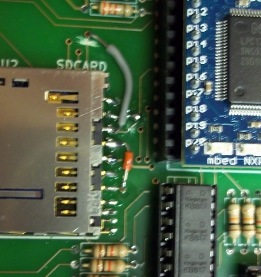
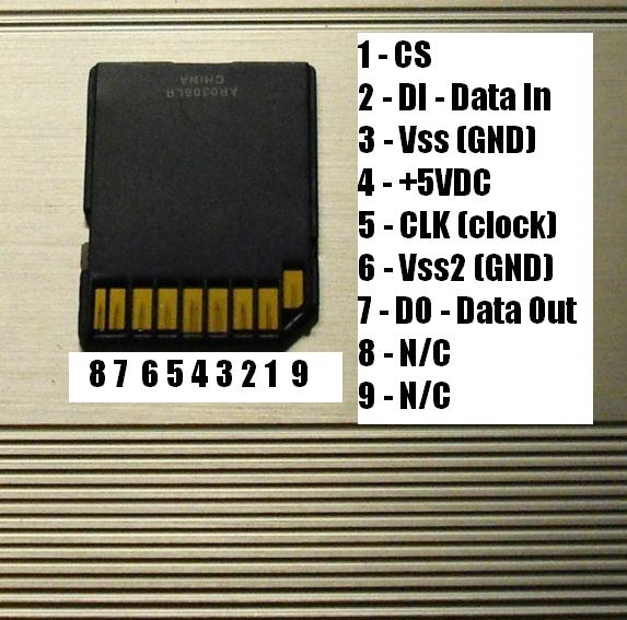
- The pads of the SD socket are placed slightly too close too far from the socket. They should be moved 0,5 mm into the socket.
- Three pins are swapped:
- PIN 1, chipselect, is now not connected but should connect to p14 on the MBED
- PIN 2, MOSI, is now connect to p14 but should connect to p11 on the MBED
- PIN3, GND, is now connected to p11 on the MBED but should bridge to PIN6
Note that the pin order is a bit strange: Pin 9 is the first Pin, next to Pin 1, and is not in use!
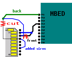
Workaround:
- On the top side of the board, cut the track from SD pin 2 to MBED p14 near SD pin 2
- On the top side of the board, cut the track from SD pin 3 to the VIA that leads to MBED p11
- On the top side of the board, connect SD pin 1 to the track that used to go to SD pin 1 (so SD pin 1 now connects to p14)
- On the top of the board, solder a bridge from SD pin 3 to SD pin 6.
- On the top of the board, solder a wire from the VIA that leads to MBED p11 to SD pin 2
- updating part file in KiCAD
- Pin 1 SD (Chipselect) connects to p14 MBED (was N/C)
- Pin 2 SD (Data In) connects to p11 MBED (was p14)
- Pin 3 SD (-Vss/GND) connects to GND (was p11)
- Pin 4 SD (VCC) connects to +5V (was ok)
- Pin 5 SD (CLK) connects to p13 MBED (was ok)
- Pin 6 SD (-Vss2/GND) connects to GND (was ok)
- Pin 7 SD (Data Out) connects to p12 MBED (was ok)
- Pin 8 SD - N/C
- Pin 9 SD - N/C
USB Connector
The holes of the USB connector are not pretinned on the bottom side of the board. This is probably a mistake in the USB connector component drawing.
Workaround: Since the pins are pretinned inside the holes, the connector will work. Just doublecheck your soldering!
H4. Ethernet
Network connector J4 is available in different types from different vendors. Pinning is different between these types.
The pin-out of this board is made for the MAGJACK SI-60002-F connector (Farnell), not for the HALO HFJ11 that is on the part-listing!
  status: need to update the BOM. No PCB change required
  MagJack  HALO    PCB modification if you want to use HALO
  p1 RD+   TX+     RD+ (OK)
  p2 VC    TX-     RD- (from MBED pin RD-)
  p3 RD-   RX+     TD+ (from MBED pin TD+)
  p4 TD+   VC      VC  (from original connection to p2)
  p5 VC    VC      VC  (OK)
  p6 TD-   RX-     TD- (OK)
To make your board function correctly: Use the Stewart MagJack part, or modify the board, using these 4 modifications: https://github.com/LaosLaser/Hardware/tree/master/laos-board-2/notes/notes/ (eth-mod1 to eth-mod4).
LEDS
The holes of ALL LEDS are not pretinned on the bottom side of the board. This is probably a mistake in the component drawing.
Workaround: Since the pins are pretinned inside the holes, the connector will work. Just doublecheck your soldering!
Phoenix connector holes
The holes for the Phoenix connectors are too small (all of them!). They are now 1mm (?) but the pins are 1mm squares, so the size should be 1.5mm.
Workaround: Use a file to make the pins round, then they will fit
Resistors
Some mistakes in resistor values:- R23, R24,R26,R27 should be 1K
- R28, R29, R31, R32 should be 330R
- R2, R3 should be 1K
- R7,R8 should be 2K2
Resistors should be renumbered so it's easier to find them on the board
Capacitors
C7 has a non-standard value (33nF), so change it to 22nF.
POLOLU J17
Pin 1 from POLOLU J17 (ENABLE) connects to MBED P20, but it should not. It should be connected to all the other POLOLU ENABLE Pins.
Workaround: On the top side of the baord, cut the track going from POLOLU J17 pin 1 near pin 1. On the top side, connect Pin 1 to the track going to all other Enable pins (it's 4mm to the right of pin 1).
Enable Solder Pads
The Enable solder pads (under the Pololu's) Connect to Pololu pin 2 (MS1), but they should connect to Pin 1 (ENABLE). Also, in the Schematic, the names of the solder pads (EN / DIR) are swapped.
Workaround: If you are using Pololu's this is not a problem at all. If you don't use Pololu's, bridge Pin1 and Pin2 of the Pololu headers with a wire.
Plus / Ground signs
Where possible, ground and +V should be marked on the print. Some obvious examples:- J38 (Power in)
- J5 (VMOT in)
J10 (I2C)
The middle two pins should be swapped to make a flat cable to the LCD/Keyboard
Workaround: Swap the pins in the wire from J10 to the LCD/Keyboard
Ground circuit of Power 5V IN
The ground of the Power 5V IN circuit is not connected to the main ground. This should be the same NET
Workaround: Scratch the GND around the power connector GND (pin 2) and make a solder connection between the two GND's
MBED Pin Vin
MBED pin Vin is connected to the Net +5VD, but this Net should not exist. This pin should be in the +5V Net.
Workaround: Use a jumper wire on the back to connect MBED Vin to the solder pad J3 (Vusb). Connect it to the +5V without joining the solder pad!
Missing jumper near J5
There should be a jumper pad to connect Pin 1 of J5 (VMOT, Stepper driver power) to VAA.
*Workaround: To get +5V on VMOT, connect a jumper wire from connector J2, pin 1, to connector J5, pin 1.
Resistor R12
The value of Resistor R12 is very dependent on the function of J14 and the value of VMOT, because a wrong value could blow up p19 on the MBED! We use it with switch to detect Lid Open/Close with VMOT=5V. In that case it should be 22K, so p19 is about 3.4V when J14 pin 3 is not connected.
Network connector
J4 p11 was connected to p18 on MBED for no reason.
status: removed line in schema and pcb rev 0.2
Bugs we noted but are not show-stoppers
Phoenix connector spacing
The outline of the Phoenix connectors is not in the component drawing. Because of that, they are places too close on the board, both too close together and too close to other components (the SD card). Because of this, it is not possible to place all Phoenix connectors on the board at the same time. This affects the location of the connectors: J9, J18, J24, J33, J37, J39, J10, J27, J14.
Workaround: This is only a real problem when you want to use all possible pins. Most lasers will not need that, so if you use 4-pin Phoenix connectors instead of 5, it will fit almost everywhere. If you really need all the pins, use other connectors, like the 2.54 spaced Phoenix mini connectors or pin headers.
7805 cooler
There should be some space around the 7805 so it can have a cooler attached.
Workaround:- Put the 7805 slightly higher or bend the cooler in between the components
- Use alternative to 7805 that doesn't get so hot:
http://letsmakerobots.com/node/3905
http://dimensionengineering.com/DE-SW050.htm?gclid=CMD26bLgq6sCFcGCDgodN3io6w
Not enough current to drive Enable on steppers
Apparently the MBED does not deliver enough current to drive the Enable on all steppers from one pin.
Workaround: An amplifier (BC-547C) should be placed just after MBED p7.
Differences between Rev1 and Rev2
- SDcard rewired to fix bugs
- Pololu microstepper resistor values updated
- Pre-tinning of several holes in the print fixed
- Ethernet connector is now always Steward Magjack, see BOM
- Hole size for Phoenix connectors fixed
- Resistor values updated
- Fixed pololu enable line for J17
- Fixed pololu enable solder pads
- Fixed disconnected ground lines
- Fixed 5V net for mbed
Differences between Rev2 and Rev3
Missing Vsensor on endstops
In Rev2, the lines marked Vsensor on J29 and J34 and the + side of the opto-couplers are connected with each other, but somehow the connection to the rest of the Vsensor net has gone missing. They should have been connected to Vsensor on J27 and the middle pin of the VCPU/Vsensor/+5V jumper. In Rev3 this problem has been fixed. Vsensor on J27 now has it's own jumper to select the power level.
CAN bus not working
In Rev2, there are a few problems with the CAN bus connection.- U1 pin 8 (Rs) should be connected to GND
- U1 pin 4 (Vref) should be left open
- U1 pin 3 (Vdd) should be connected to 5V (instead of 3V3)
This has been fixed in Rev3
Swapped label for Direction and Enable
In Rev2, the (E)nable and (D)irection pin labels are swapped in the design and on the PCB markings. It does not cause functional problems, as long as you make sure your wiring of external drives is correctly connected. In Rev3, this has been fixed.
Series resistor for analog input
In Rev3, an extra resistor (R33) was added between AIN (PIN 3 of J14 and the junction of R10/R12. This allows us to make a voltage divider. Typical value for R33 should be 1K.
Series resistor for analog output
In Rev3, an extra resistor (R34) was added between the MBED and AOUT (PIN 2 of J24), in order to limit currents in case of a ground connection of the analog output.
Solder joints for Pololu microstep factor
Instead of jumpers, Rev3 has solder joints so it is easier to solder the pins to +V to obtain microstepping. Solder joints: J7, J16, J22 and J31
Moved Ethernet connector
In Rev3, the Ethernet connector has been swapped with the USB to allow easier connection of the MiniUSB connector of the MBED.
Added FFC / FPC connector
Rev3 has place for a FFC / FPC connector, as used in some HPC and Chinese Lasers. This connector combines X-Axis stepper and endstops.
Updated by jaap about 13 years ago · 4 revisions