Forums » Hardware development »
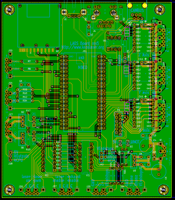
 Upcoming rev 5 mainboard
Added by Springuin about 12 years ago
- Schematic cleanup
- Removal of unused components (E-axis)
- Different location of diverse connectors for more straightforward layout
- Differential routing for USB and ethernet signals
- Ethernet connector and SD card socket on the same side of the PCB
- All power related connectors on the right side
- All opto's and endstops on the bottom
- All other connectors on the left
I just checked in my working version. I'm not completely finished but the routing is complete. I want to do some more fine adjusting/polishing.
Kicad data is in https://github.com/LaosLaser/Hardware/tree/master/laos-board-rev5
A picture is attached to this post.
Any suggestions, things that can be improved? Please let me know what you think!
Replies (9)
 RE: Upcoming rev 5 mainboard
-
Added by KalleP about 12 years ago
RE: Upcoming rev 5 mainboard
-
Added by KalleP about 12 years ago
Looking very good.
A lot of good improvements already implemented and the engineering feels right, a few suggestions and observations.
The board hole layout should be an a rectangular grid, if you want to support the old funny corner hole then rather use a slot for the one corner.
The CAN bus is often intended to be used on internal features so also having a connector that faces inside could be useful.
I vaguely remember an old thread that mentioned the CAN bus RJ12 pinout was mirrored/non-standard, not sure which revision that was.
A top facing reset button on the SD card edge would be an assistance to debugging if the button on the MBED is hard to reach, perhaps on the solder side of the PCB under the SD card (SMD so no holes under SD card socket if required) as an option when using the SD card to update configs.
Having both +5V and GND signals near the opto terminals would be very useful sometimes when connecting to other opto IO or making pull-ups and filters for laser power control.
The cyan text on green in the photo is impossible for me to read (a type of, perhaps rare, colour blindness) so I cannot offer suggestions on the legends until I load KiCAD or edit the preview PNG
I would feel better if the ground-plane was not broken between the stepper drivers (a wire/resistor link would be acceptable to avoid it), having a good earth is a plus around power devices.
I cannot see if the extra Pololu electrolytic capacitors are supported.
The extra jumpers/links and terminals for gnd/power at the stepper output terminals are not needed if the jumpers/links to run the step/dir/en signals through are not supported. A more generic solution might be to have a little carrier board with a Pololu pin layout that has takes all the required signals to a suitable terminal or connector (using some popular industry standard [gecko?]) on the carrier board.
The LEDs would look real neat if all in a row (even one next to each stepper driver would be OK).
None of these are mission critical and would not stop me using rev5 but might help some people out.
I like it.
RE: Upcoming rev 5 mainboard
-
Added by Springuin about 12 years ago
Thanks for the comments. I appreciate them.
The board hole layout should be an a rectangular grid, if you want to support the old funny corner hole then rather use a slot for the one corner.
I'll see if I can make it a slot hole
The CAN bus is often intended to be used on internal features so also having a connector that faces inside could be useful.
I agree; however: currently there is no can bus support, so it is not really used. Instead of a right angled connector one could also use a straight connector or wires to keep it on the inside. There is not much room for another solution or to put it somewhere else on the board so I'll leave it for now.
I vaguely remember an old thread that mentioned the CAN bus RJ12 pinout was mirrored/non-standard, not sure which revision that was.
Yes, but that depended on which connector and how you looked at it. I've chosen a connector (Molex 95501-2641) and corrected the footprint for that.
A top facing reset button on the SD card edge would be an assistance to debugging if the button on the MBED is hard to reach, perhaps on the solder side of the PCB under the SD card (SMD so no holes under SD card socket if required) as an option when using the SD card to update configs.
In such case I suggest connecting a button directly to the pins of the mBed.
Having both +5V and GND signals near the opto terminals would be very useful sometimes when connecting to other opto IO or making pull-ups and filters for laser power control.
The endstop connectors next to the opto connectors have Vendstop (+5V, VMOT or VCPU) and GND.
The cyan text on green in the photo is impossible for me to read (a type of, perhaps rare, colour blindness) so I cannot offer suggestions on the legends until I load KiCAD or edit the preview PNG
I was not yet finished with the silkscreen text.
I would feel better if the ground-plane was not broken between the stepper drivers (a wire/resistor link would be acceptable to avoid it), having a good earth is a plus around power devices.
I already saw that, it's fixed now.
I cannot see if the extra Pololu electrolytic capacitors are supported.
They are, and they are to be mounted under the drivers.
The extra jumpers/links and terminals for gnd/power at the stepper output terminals are not needed if the jumpers/links to run the step/dir/en signals through are not supported. A more generic solution might be to have a little carrier board with a Pololu pin layout that has takes all the required signals to a suitable terminal or connector (using some popular industry standard [gecko?]) on the carrier board.
External stepper drivers are still supported; by placing bridges instead of the pololu stepper driver. I think I'll bridge the GND jumper by default and remove the VMOT bridge.
The LEDs would look real neat if all in a row (even one next to each stepper driver would be OK).
None of these are mission critical and would not stop me using rev5 but might help some people out.
 RE: Upcoming rev 5 mainboard
-
Added by arc310 almost 12 years ago
RE: Upcoming rev 5 mainboard
-
Added by arc310 almost 12 years ago
- Silkscreen : on my rev4 board, SDA an SCL were swapped on the silkscreen : GND SCL SDA 5V (compared to the panelboard : GND SDA SCL 5V), but the pins were OK (ie no swapping required to make the cable between laosboard and panelboard)
- The flatcable : pin 1 and 6 (GND) had to be connected for the connection to work (with my rabbit HX3040)
Thanks for the good work !
RE: Upcoming rev 5 mainboard
-
Added by Springuin almost 12 years ago
Silkscreen is fixed; flatcable: ok, I'm leaving that now for backward compatibility. I currently have a test version of the rev 5 board and just ordered the parts to test the board.
 RE: Upcoming rev 5 mainboard
-
Added by jaap almost 12 years ago
RE: Upcoming rev 5 mainboard
-
Added by jaap almost 12 years ago
Flatcable: it's the first time I hear about it, so please don't fix: apparently the Rabbit HX3040 needs something else then the HPC-3020 (which is our reference model).
RE: Upcoming rev 5 mainboard
-
Added by arc310 almost 12 years ago
About the flatcable : it is actually just what is show here : http://redmine.laoslaser.org/attachments/download/89/HPC-flat-cable-pinning.jpg
Maybe the HPC-3020 has the two grounds already connected together at the other end of the flatcable ?
 RE: Upcoming rev 5 mainboard
-
Added by reinoud almost 12 years ago
RE: Upcoming rev 5 mainboard
-
Added by reinoud almost 12 years ago
Please leave the flatcable intact! Our machine, a Chinese K-III has a flatcable that just fits :) It would otherwise take a lot to split it all up again.
RE: Upcoming rev 5 mainboard
-
Added by Springuin almost 12 years ago
The flatcable pinout has not changed in rev 5; it worked in older revisions and it's easier to make than to break a ground connection.