Forums » Hardware development »
 Display board design, time for update?
Added by jaap almost 13 years ago
I ran out of PCB's for the display board. I could just order a new batch from the manufacturer, but maybe there are improvements we should make? Any ideas?
Replies (16)
 RE: Display board design, time for update?
-
Added by hugomeiland almost 13 years ago
RE: Display board design, time for update?
-
Added by hugomeiland almost 13 years ago
just some thoughts...
- how about easier to solder connectors?
- check heights of display and buttons
- new joystick, for which a button can be found
- integrate some safety functions like:
-- check for waterflow
-- temp of laser
-- lid sensor
or the other way round and use something like this: http://dx.com/p/lcd-keypad-shield-for-arduino-duemilanove-lcd-1602-118059
Hugo
 RE: Display board design, time for update?
-
Added by peteruithoven almost 13 years ago
RE: Display board design, time for update?
-
Added by peteruithoven almost 13 years ago
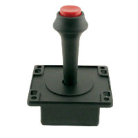
About the joystick, what about:
http://na.suzohapp.com/images/50/50800010.jpg
http://na.suzohapp.com/images/50/50700800.jpg
No seriously, where can you get simple 4 way joystick buttons, I've bin looking for them. Something like:
http://www.miniinthebox.com/replacement-spare-button-kit-for-psp_p156604.html?pos=ultimately_buy_3
http://www.miniinthebox.com/replacement-3d-analog-joystick-buttons-for-psp-black_p346490.html
Something like you find on controllers:
http://upload.wikimedia.org/wikipedia/commons/8/83/NES-controller.jpg
http://www.emtcompany.com/style/images/products/41ea618c758995d32ef97dfd2b0a6914.jpg
http://www.digitaltec-ba.com/loja/images/6646.jpg
Or maybe this remains something to 3D print.
 RE: Display board design, time for update?
-
Added by Springuin almost 13 years ago
RE: Display board design, time for update?
-
Added by Springuin almost 13 years ago
Jaap, I've looked at the PCB design and have the following suggestions:
- Put the most of the traces on the front layer and the GND plane on the back layer. Also, the clearance of the ground plane can be much smaller.
- Make all traces either horizontal, vertical or 45 degrees; there is no technical reason to do this with this kind of PCB, but it just looks nicer and more professional.
- Replace the BC547 and 680Ohm resistor with an N-fet, something like BS270 is just fine. Transistors are for amplifiers, a FET is more suited for just switching, plus you don't need a resistor.
- Make use of labels in the schematic; the connections between the ATmega and the display is really hard to follow.
- Put U1 closer to the VCC and GND pins of the atmega. Next to F1 or next to P9 is much better.
- Add a regular AVR ISP connector, the 6 pin one with MISO, MOSI, SCK, RESET, GND and VCC. This makes debugging using an AVR dragon much easier
- Use one normal sized (12.5mm) resistor shape for all resistors, there is no particular reason but it looks nicer.
- Use via's instead of one-pin connectors
- Give P2 more room so a JST connector or something alike would fit on the pcb
- Use the flip function to put components on the right side of the board. The current board has all components on the top layer while actually the lcd, buttons and joystick are on the back.
For backward compatibility:
- Do not move the joystick, buttons, mounting holes or display
If you want I can do the design the way I think it should be or you are welcome to come over and we do it together.
RE: Display board design, time for update?
-
Added by Springuin almost 13 years ago
I'm playing with the layout of the board and schematic and have two questions:
- why are the mounting holes surrounded by 6 small holes?
- where is jumper P7 used for?
 RE: Display board design, time for update?
-
Added by parag0n almost 13 years ago
RE: Display board design, time for update?
-
Added by parag0n almost 13 years ago
Should i2c slave devices have some sort of pullup resistors on them to make the connection work properly? I'm having occasional dropouts on my i2c board where the LCD stops responding, was wondering if maybe the lack of pullups on the i2c board is effecting them somehow?
RE: Display board design, time for update?
-
Added by Springuin almost 13 years ago
For I2C you need a pullup resistor on SDA and on SCL, one on each line for the whole bus. In this case the resistors are on the main board (R7 and R8) so that's fine.
However, I wonder if a level converter is neccesary; the mbed is a 3.3v device, the ATmega runs on 5V and the pullups are connected to 5V but that does not necessarily mean that the bus runs on 5V. Parag0n, can you measure the voltage on SDA and SCL for me when there is no communication?
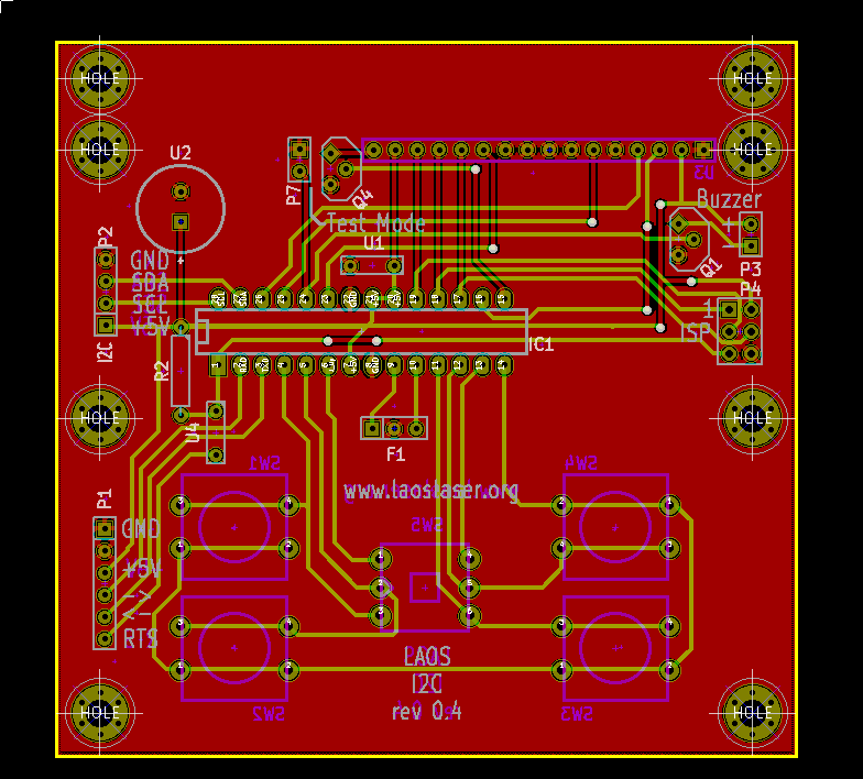
Yesterday I made a new layout, see https://github.com/Springuin/LaosLaser-AddOns/tree/master/i2c-panel/pcb-0.4 for a preview. When I'm satisfied I will issue a pull request.
Hugo, "easier to solder connectors"? What do you mean by that? Larger pads?
RE: Display board design, time for update?
-
Added by hugomeiland almost 13 years ago
Hugo, "easier to solder connectors"? What do you mean by that? Larger pads?
The board side is fine; I was referring to the cable side; the current connectors are a pain to crimp without the right (150euro+) tools. Using easier connectors might make this easier for diy's.... another option would be to provide pre-crimped cable assemblies...
could you provide a pdf version of the board?
thanks!
Hugo
RE: Display board design, time for update?
-
Added by Springuin almost 13 years ago
Nice, easy crimpable 2.54mm pitch connectors are Molex KK series, Harwin M20 and alike.
There are affordable crimping pliers that work with this kind of connectors called HT-225D, available from Farnell (expensive), Amazon, and Distrelec (27,45 euro ex VAT). Or you can use normal needlenose pliers, as long as you don't have to do a lot of these contacts.
Another option is to just solder pinheaders and use these wires: http://dx.com/p/30cm-breadboard-wires-for-electronic-diy-40-cable-pack-80207?rt=1&p=2&m=2&r=3&k=1&t=1&s=15234&u=80207 but they are not polarized, which can lead to smoke...
I'm not really able to get a nice pdf out of KiCad, print to file gives ugly pads, plot to svg makes the bottom layer almost invisible; the png file attached to the previous post is the best I can do.
RE: Display board design, time for update?
-
Added by hugomeiland almost 13 years ago
sorry, missed the png; looks great! what size are the mounting holes? I remember rev3 ones were 2.5; can they be made 3mm, that size screws is much more common on stock....
I'm very much in favor of using polarized connectors! Can the jst connectors also be crimped with the HT-225D tool? or is there an other tool available for a reasonable price??
thanks! Hugo
 RE: Display board design, time for update?
-
Added by KalleP almost 13 years ago
RE: Display board design, time for update?
-
Added by KalleP almost 13 years ago
I have a few thoughts.
- I second the increase in mounting hole size to 3mm
- A further set of mounting holes beyond the LCD holes might be of value to allow for the same length standoffs for the board corners and allow premounting the LCD to the correct height to match the through/behind panel position. Leave the holes from the rev 0.3 position for backward compatibility
- Hole sizes were a bit tight on the rev 0.3 for the joy button (I almost destroyed mine when moving it to the correct side of the PCB)
- A jumper to enable local test mode (or use JP7 if it is not used for other function) would allow for stand alone testing with pre-loaded production firmware.
- A option for a transistor and a buzzer perhaps shared with the jumper pin (jumper to +5V = test mode, jumper to buzzer drive transistor base = buzzer mode)
Good work so far, my project was packed away for our house move, hopefully time to unpack it again soon.
RE: Display board design, time for update?
-
Added by Springuin almost 13 years ago
Hugo, the HT-225D crimps most standard pins for wires with size 18-30 awg, so I assume JST connector pins work just as well; if you like I can bring it to the makerfaire, so you can see for yourself.
I increased the holesizes for the joystick. They now match the datasheet.
I think a jumper for test mode is a good idea; P7 is not used, as far as I can see. This also makes it possible to make pre-programmed microcontrollers that don't require reprogramming.
About the buzzer: anyone else an opinion on that?
Jaap, is it an option to make the board a little larger, say 10mm on all sides?
Can someone measure the voltage on de SDA and SCL lines for me so I can determine if a I2C level converter is a good idea?
RE: Display board design, time for update?
-
Added by KalleP almost 13 years ago
I proposed the buzzer so it can alert the operator when he is working on the next layout onthe other side of the room.
The two things I can think of at the moment are a limit exceeded (due to lost steps), cooling/fan/air assist failure or a flame detector indication. Secondly for those who have manual lasers that require user adjustment of the laser power or the Z-height (to cut through thicker materials or that cool out of focus heating technique used to bend plastic) the buzzer could request user intervention. Also it could signal job complete even before the fan is turned off to maximise production time.
RE: Display board design, time for update?
-
Added by Springuin almost 13 years ago
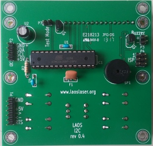
I added the buzzer; the way it's now you can put a jumper on P7 for debug mode; on startup the software can check for the existence of the jumper (enable pullup on PC1); if there is a jumper (PC1 low) then go in debug mode. If there is no jumper the pin can be used as output to control the FET that switches on the buzzer. This does not break backward compatibility.
I2C levelshifter is not neccesary; I measured the I2C voltage on an existing mainboard: the pullups to 5V together with the 5V tolerant inputs on the LPC1769 pull the SDA and SCL up to 5V, so that's fine.
I enlarged the PCB to provide enough space for the larger mounting holes and to make room for two extra mounting holes above the display; so you can mount the display on the PCB using 4 screws and spacers and then there are 4 more holes to mount the PCB to backside of the front panel.
All holes are now sized for M3 screws; I know that LCD's like the one used here usually have holes for M2.5 but 3.35mm holes are not too large for M2.5 screwheads and M3 is easier to get.
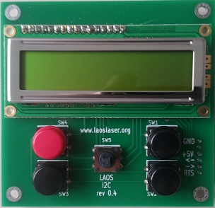
Picture of the board is attached
RE: Display board design, time for update?
-
Added by jaap almost 13 years ago
Just pulled your changes in on Github. Thank you Springuin!
RE: Display board design, time for update?
-
Added by KalleP almost 13 years ago
New layout looks good. A few suggestions though sorry for so many, mostly optional changes.
Any chance you could also route the buzzer trace to the area above SW4 or in the free space above the LCD. It would allow soldering the buzzer at the back of the PCB where it is usually out of the way. I would also put in holes 0.1, 0.2, 0.4" apart to accommodate a couple of different types of buzzer pin spacing.
Kind of clever idea with the test mode jumper detection. If I understand correctly you would use the internal pull-up to drive the MOSFET and output a low to turn off the buzzer. When you do the power on beep you would read the port pin and check if it is grounded through the jumper. If so then this is very cunning but will fail if someone uses a bipolar transistor instead as it will clamp the voltage to 0.7V. I think a more robust suggestion of a 2 way (3 pin) jumper might be the way to go with a pull down resistor on the transistor to measure low when in run mode and the jumper to +V for test mode.
Place for an optional diode across the buzzer (some of those small ones are like a car hooter) might be welcome if someone uses it to drive a larger fire alarm relay or siren one day.
Jumper should be in a position to be accessed from the front or back (not trapped behind the LCD), a popular position I have seen is near the edge of the board, it would allow use of right angle pins to access from a side if space behind board is limited in some application and front is behind panel.
I want to get my local situation so that I can actually do schematic editing on project files so I can make changes instead of making work for others but it will have to wait for a couple of things to settle down first.
Kalle
--
Johannesburg, South Africa
RE: Display board design, time for update?
-
Added by jaap over 12 years ago
Hi people,
Thanks for all your input!
And special thanks to Springuin, for updating the design.
The new version v0.4 is now available from me.